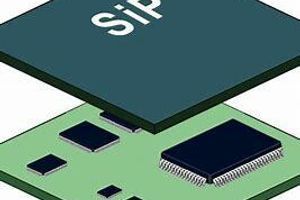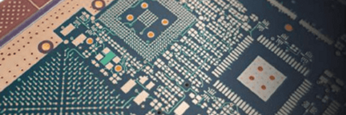
Modern methods of mounting integrated circuits allow for significant size reduction, increased performance, and improved heat dissipation.
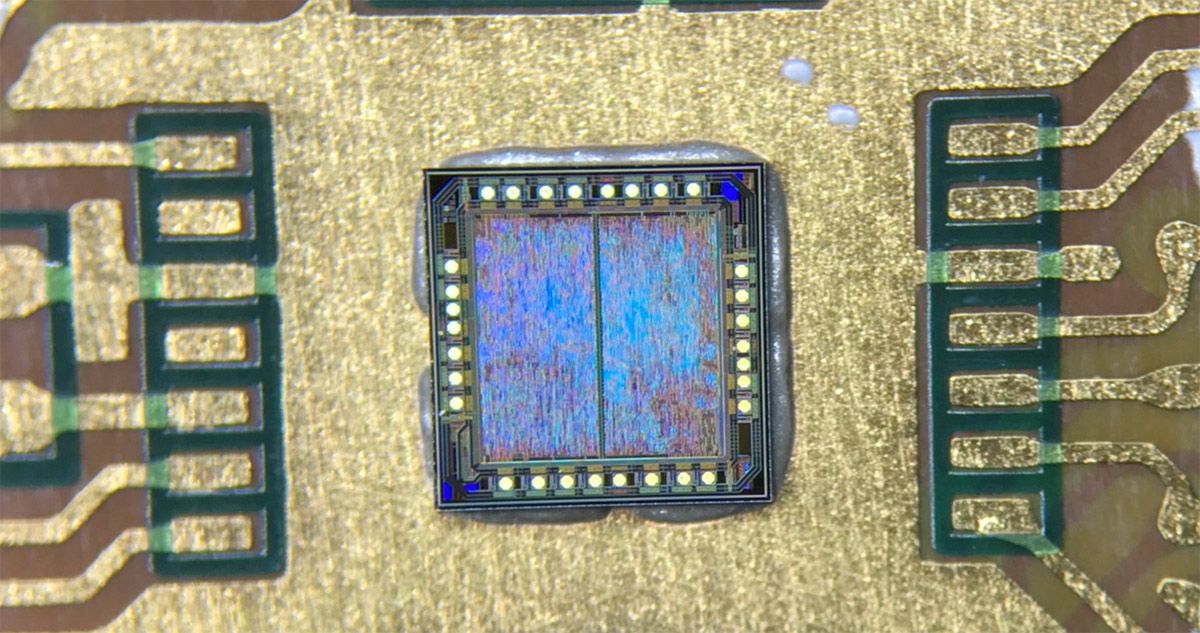
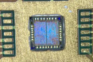
A tiny bare die chip is placed on a printed circuit board using a precise and advanced electronic assembly process.
Ball Grid Array (BGA) Technology
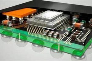
Ball Grid Array (BGA) is a popular technology that uses solder balls instead of traditional leads, allowing for an increased number of connections and improved mounting reliability.
Wafer Level Chip Scale Package (WLCSP)
Wafer Level Chip Scale Package (WLCSP) is an even more compact approach, where the chip packaging is done directly at the wafer level. This enables minimal device dimensions while maintaining high performance.
BGA Package Structure
A BGA package consists of a protected top and an open bottom side with a solder ball grid.

The grid layout ensures that each solder ball forms a connection between the printed circuit board and the BGA package. As a result, BGA mounting reduces the overall system size while simultaneously enhancing system performance.
Thanks to these methods, manufacturers can develop miniaturized yet powerful electronic devices.