Author: Nadya Lukman
The Future of Miniaturization and Breakthrough Technologies: PoP, SiP, TSV, EMIB
The reduction of transistors to the nanometer scale faces physical limitations, driving the search for new approaches. Research is advancing in the fields of organic transistors, quantum computing, and nanomaterials. For example, graphene-based transistors and carbon nanotubes could enable even smaller sizes and higher efficiency. Quantum computers, which utilize quantum bits (qubits), have the potential to revolutionize computing.
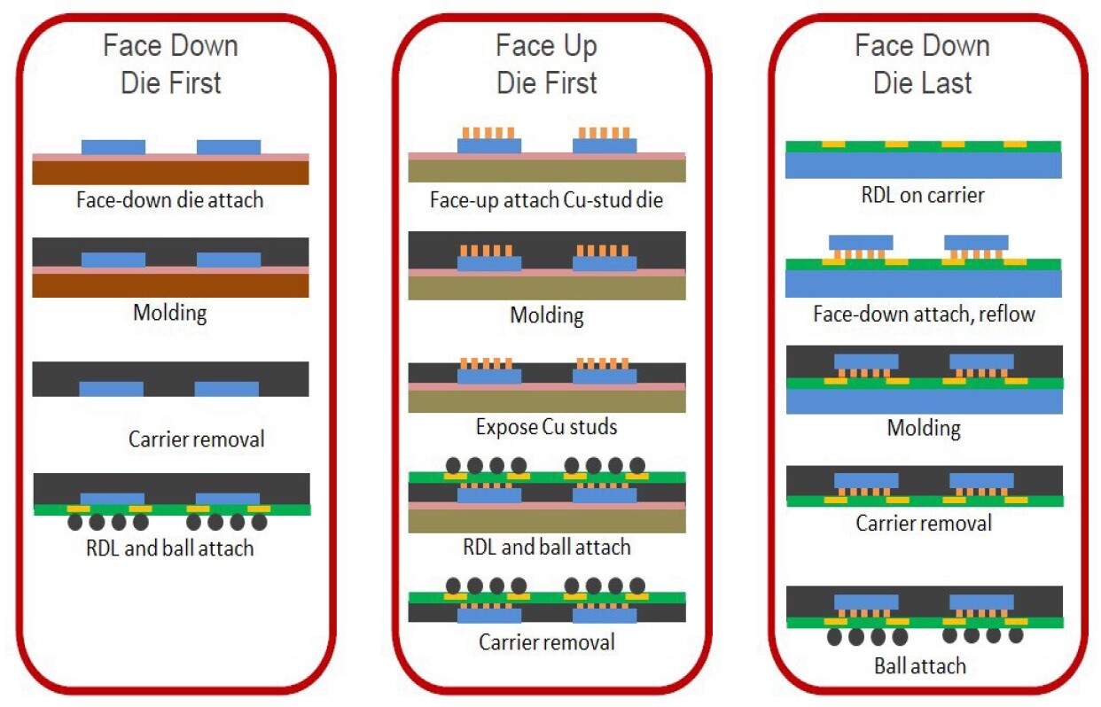
Additionally, cutting-edge semiconductor packaging technologies are being actively developed, including Package on Package (PoP), 3D System-in-Package (SiP), Fan-out Wafer Level Packaging (FOWLP), Through-Silicon Via (TSV), and Embedded Multi-die Interconnect Bridge (EMIB).
Package on Package (PoP)
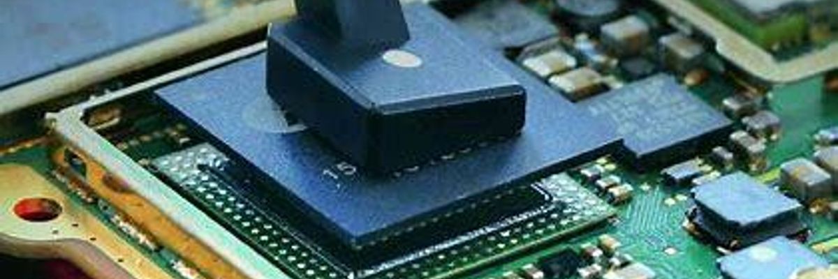
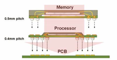
PoP technology allows for the efficient integration of multiple chips, typically stacking a memory package (such as mobile DRAM) on top of a processor package. This optimizes space, enhances performance, and improves thermal management. PoP is widely used in smartphones, tablets, and networking equipment.
3D System-in-Package (SiP)
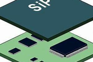
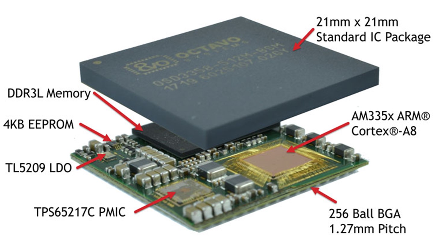
SiP enables multi-layer vertical stacking of components within a single package, reducing device size while increasing functionality. It is utilized in IoT devices, automotive electronics, and high-performance computing.
Fan-out Wafer Level Packaging (FOWLP)
FOWLP technology extends contact pads beyond the active chip area, reducing package thickness and improving thermal performance. It is ideal for wearable devices and high-performance computing systems.
Through-Silicon Via (TSV)
TSV enables vertical electrical connections through the silicon layer, increasing data transfer speed and reducing signal delays. It is commonly used in 3D-stacked memory and advanced processors.
Embedded Multi-die Interconnect Bridge (EMIB)
EMIB efficiently integrates multiple dies within a single package using an embedded interposer. This provides high bandwidth and low power consumption, making it ideal for servers, data centers, and AI accelerators.
These breakthrough technologies enable the development of even more compact, powerful, and energy-efficient electronic devices, paving the way for a new era of miniaturization and integration in electronics.