The AI Era, Oversized BGA Packages, and New Challenges for SMT Assembly
It’s incredible how quickly the world of electronics is changing under the influence of Artificial Intelligence (AI)! 🚀 AI was once a topic confined to research labs, but today it demands a radical re-evaluation of our manufacturing processes, especially in Surface Mount Technology (SMT).
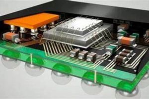
The rapid penetration of AI into all sectors—from high-performance servers and autonomous vehicles to industrial equipment—has introduced absolutely new, extreme requirements for physical design. To deliver the massive computing power needed, microchips that simply didn't exist before are required: Oversized Ball Grid Array (BGA) packages.
📈 Trend: From a 40x40 mm Chip to a 150x150 mm Monster
Traditionally, most SMT lines were capable of handling processors and chipsets up to 40x40 mm or 50x50 mm. That was the standard. However, chips designed for modern AI systems (GPUs and specialized accelerators) can reach dimensions of 100x100 mm or even 150x150 mm (Multi-Chip Modules, MCMs).
These "giants," weighing up to 500 grams and featuring tens of thousands of pins, require Multisize Placement technology.
Why Are They So Large?
-
Multi-Chip Modules (MCM): The use of several interconnected dies (chiplets) on a single substrate to increase computational density.
-
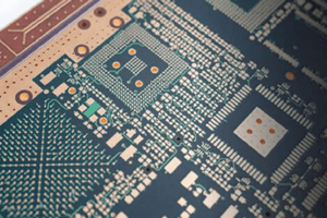
High Pin Count: Over 20,000 solder balls are needed to ensure ultra-high data throughput.
-
Heat Dissipation and Weight: Massive integrated heat spreaders increase the weight to up to 500 grams, requiring specialized handling.
⚙️ Technological Challenges for Contract Manufacturing
Processing these "giants" transforms standard SMT assembly into a process that demands advanced technologies:
-
Precision and Placement Force: Specialized equipment with Very High Force capabilities and mechanical stability is required for ideal placement of heavy components.
-
Visual Inspection (MFOV): Multiple Field of View (MFOV) technology is necessary for precise centering of chips with thousands of pins, which is impossible with traditional methods.
-
Specialized Tooling: Custom-adapted nozzles must be used to pick up large and fragile BGAs without causing damage.
⚠️ Risks for Traditional EMS Companies
For contract manufacturers whose lines are limited to the traditional 40–50 mm size, the emergence of oversized BGAs creates significant risks:
-
Technological Obsolescence: Existing equipment becomes incapable of processing key components in the fastest-growing market segment (AI/HPC).
-
Loss of High-Margin Orders: Projects in AI and 5G are among the most profitable. The inability to perform Multisize Placement blocks access to this niche.
-
Need for Capital Investment: Modernization requires significant expenditure on new, high-precision machines and X-ray inspection systems.
🔭 Where Are Giant BGAs Already Used and Penetration Forecast
Oversized BGAs/MCMs (100–150 mm) are already the standard in areas where performance is critical:
Current Application Areas:
-
Data Centers/Cloud Computing: Processors for training large language models (LLMs).
-
High-Performance Computing (HPC): Main computing nodes in supercomputers.
-
Network Infrastructure: High-speed 5G/6G switches and routers.
Penetration Forecast: Replacement of Traditional Chips

💸 Economic Feasibility: Is the Replacement Worth It?
At first glance, manufacturing an oversized BGA chip (150x150 mm) seems much more expensive than using traditional, smaller solutions. Indeed, the production of these giants, with their complex multi-layer substrates, often results in a lower component yield, which sharply increases their price.
But here, we must look beyond the cost of a single component and consider the economics of performance at the system level.
For me, this is not a question of cost-effectiveness, but of unavoidable necessity. We simply cannot build an autonomous car or train the newest large language model (LLM) using a collection of dozens of traditional chips. It is technically impossible due to prohibitive latency, required power, and inefficient use of board space.
An oversized BGA package is essentially a compact supercomputer. Its high cost is justified by savings in system integration: one such chip replaces several complex boards, reduces the number of PCB layers, and simplifies the power and cooling systems. Ultimately, the high chip cost is offset by an extraordinary gain in performance and a reduction in the overall complexity and size of the end device.
However, it is important to remember that this revolution will not affect most market segments. I believe it is highly likely that production technologies for the vast majority of electronic products will not change in the coming years. Your smartphone, TV, or industrial controller will continue to use traditional chip sizes that are easily mounted on standard SMT lines. Heavy-duty chips will remain a niche industry—they will be servers, AI accelerators, and autonomous control systems. Therefore, most traditional EMS companies not targeting this high-end segment do not face an immediate rush to buy the most expensive equipment. But keeping this technology on our radar, as we are doing, is the key to being ready for the future.